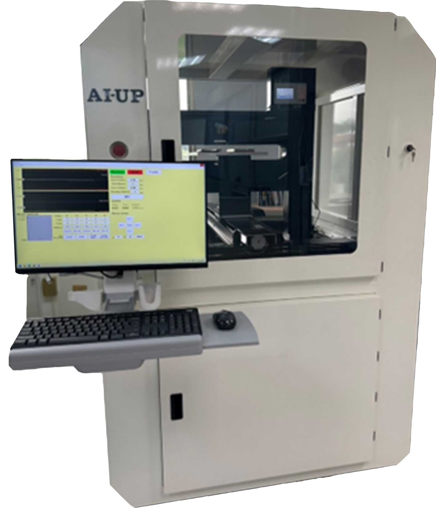
高精度雷射晶圓檢測系統
Laser Wafer Inspection Equipment
Dual Laser Measurement
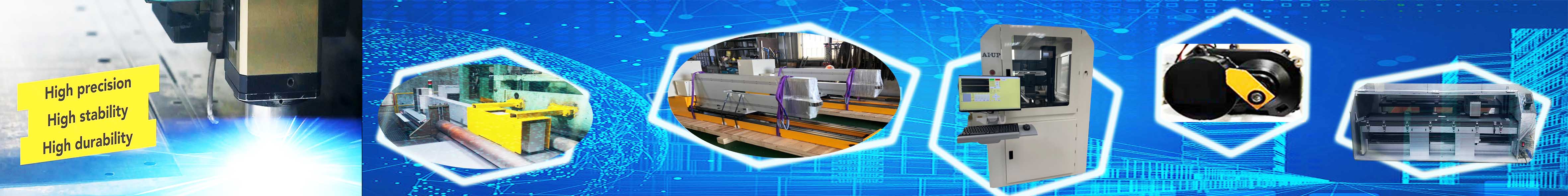
- High precision (μm)
- Non-contact dual laser
- High-speed dynamic measurement
- User-friendly software interface
- High stability and reliability
- Thickness, TTV, Bow, Warpage measurement
- Data record
"Laser Wafer Inspection Equipment" measures thickness,TTV, Bow and Warpage at the same time with micron (μm) accuracy. It combines precise algorithm and high precision, high stability lasers. It also has the benefits of non-contact, instant monitoring, continuous measuring and no radiation damage. The core technology development is based on the existing non-contact dual-laser inspection system (AI-UP's core patented technology), and uses the SECS specification. To combine real-time measurement values with ERP or MES system, it can contruct a real-time digital integration service platform. The measurable wafer sizes include: 2-inch (50mm), 4-inch (100mm), 6-inch (150mm), 8-inch (200mm) and 12-inch (300mm) wafers.
- Wafer manufacturing
- Wafer Foundry
- Wafer Thinning
- Wafer Packaging and Testing
- Factory Automation
| AI-UP Laser Wafer Inspection Equipment | |
|---|---|
| The Laser Sensor | |
| Accuracy (um) | 0.2 |
| Resolution (um) | ±1 |
| Measuring frequency (Hz) | 10k |
| Display Resolution (μm) | 1 |
| Thickness (μm) | ±2 |
| TTV (μm) | ±2 |
| Warpage (mm) | ≦ 20 |
| The High Precision XY Tablet | |
| Move Range (mm) | 300 X 300 |
| Wafer Size (mm) | ≦ 300 |
| Repeatability (um) | ±0.5 |
| Position accuracy (um) | ± 1.5 |
| Protection class | IP65 |